
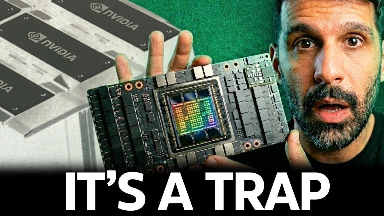
NVIDIA Absorbs Groq in a $20 Billion Move as the Chip War Shifts From Training to Inference
With inference already running two-thirds of the world’s AI compute, NVIDIA’s Christmas Eve licensing deal for Groq’s patents, software, and top engineers quietly removed its fastest challenger while AMD, Cerebras, and Tesla scatter across entirely different mountains.

Nvidia Pays $20 Billion for Groq's Team as the AI Chip War Shifts to Inference
By licensing Groq’s entire patent portfolio and hiring founder Jonathan Ross plus roughly 80% of its staff on Christmas Eve, the $5 trillion chip king is fortifying the one battlefield - inference - where in-house silicon from Google, Amazon, and Microsoft most threatens its 75% margins.
Elon Musk Just Made the Bet of the Century on Chips
Securing the entire AI supply chain with triple redundancy as Taiwan tensions escalate
The global chip industry faces its most precarious moment in decades. Advanced semiconductor manufacturing is concentrated in the hands of just three companies, one of which sits on an island 100 miles from mainland China. At the same time, demand for AI accelerators, robot brains, autonomous vehicle processors, and space-based compute is exploding faster than factories can keep up. Against this backdrop, Tesla, SpaceX, and xAI have executed an unprecedented series of moves that lock in capacity across every major foundry while building a fully vertical, US-based mega-factory capable of producing everything from raw silicon to finished AI chips under one roof.
Key Takeaways
Only three companies on Earth can manufacture the most advanced semiconductor chips below seven nanometers: TSMC in Taiwan (roughly 90% of global leading-edge output), Samsung in South Korea, and Intel in the United States.
Tesla, SpaceX, and xAI have secured dedicated production lines with all three foundries, creating triple redundancy for AI chips powering Full Self-Driving, Optimus robots, Grok training, and next-generation satellite constellations.
Terra Fab, a $25 billion vertically integrated facility on Tesla’s Austin campus, will handle the entire chip-making process—design, logic fabrication, high-bandwidth memory, advanced packaging, and testing—at massive scale, targeting 100,000 wafer starts per month initially and eventually scaling to one million.
An eight-year, $16 billion agreement with Samsung guarantees long-term capacity for the next-generation AI6 chip on the bleeding-edge two-nanometer process at Samsung’s new Taylor, Texas fab, just miles from Tesla’s Gigafactory.
US government backing through the CHIPS Act gives Intel roughly 10% public ownership, aligning national security interests with the success of the domestic foundry now partnering on Terra Fab.
AI chip demand currently runs three times higher than available supply, while high-bandwidth memory prices are projected to surge 130% through 2027, making secured capacity a decisive competitive edge.
This strategy delivers strategic insurance against potential disruption of Taiwan’s chip output, which military analysts project could trigger a $10 trillion global economic hit—worse than the 2008 financial crisis and COVID-19 combined.
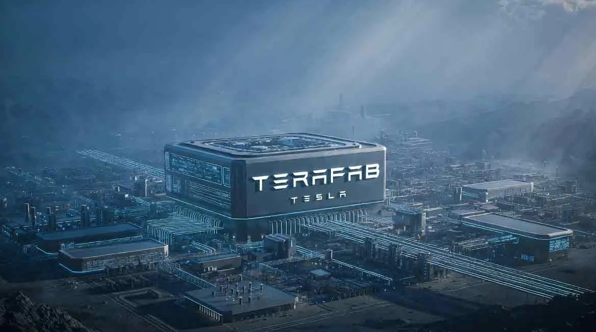
Elon Musk’s $25 Billion Chip Factory Is the Biggest Industrial Bet Ever Made
One Texas plant could crank out enough custom AI silicon to power a terawatt of compute—most of it headed to space—while rewriting the rules on design speed and efficiency.
A single factory under construction in Texas is preparing to manufacture custom AI chips at a scale that would consume more advanced semiconductor capacity than most nations currently possess. The project aims for 200 billion chips per year and one terawatt of annual compute power, with roughly 80 percent destined for orbital AI satellites launched by SpaceX. The real game-changer lies in how the factory compresses chip design cycles from months to weeks and uses advanced packaging techniques to stretch limited high-end lithography resources far beyond what traditional foundries achieve. This approach turns a seemingly impossible supply-chain bottleneck into a structural advantage for autonomous vehicles, humanoid robots, and space-based AI systems.
Key Takeaways
The factory starts at 100,000 wafer starts per month and scales to 1 million—roughly 70 percent of TSMC’s current worldwide output from all its plants combined.
Every two-nanometer chip relies on extreme ultraviolet lithography machines produced by a single company in a Dutch town of 45,000 people; global production sits at only 50 to 60 units per year, with every machine already spoken for years ahead.
In-house mask-making and rapid wafer runs shrink chip iteration cycles from three-to-four months down to one-to-two weeks, delivering five-to-ten times faster design progress than standard foundry loops.
Chiplet architecture limits expensive EUV usage to only the compute cores while sourcing memory and input/output dies on older, readily available nodes—boosting yields from 30-40 percent on monolithic dies to around 80 percent.
Custom inference silicon optimized specifically for Tesla workloads removes idle transistors, delivering major gains in power efficiency, latency, and cost—critical for extending robot runtime and lowering per-unit economics to $2 per hour of labor.
The strategy outsources heavy EUV volume work to existing foundries while owning the design-to-packaging loop, creating a compounding moat that widens each year as competitors remain locked into general-purpose chips.
Geopolitical risks around Taiwan and China’s slower EUV progress make localized, rapid-iteration capacity a strategic hedge for Western AI leadership.